

Exploring the latest advancements in semiconductor design and manufacturing processes that are revolutionizing the electronics industry.
The semiconductor industry has undergone remarkable transformations in recent years, with 2025 marking a pivotal moment in its evolution. As we navigate through this technological renaissance, it's essential to understand the key developments that are shaping the future of electronic components and systems.
The Rise of 2nm Process Technology
After years of research and development, leading semiconductor manufacturers have successfully commercialized the 2nm process technology. This breakthrough represents a significant leap forward in transistor density and energy efficiency, enabling the creation of more powerful and less power-hungry electronic devices.
The transition to 2nm has not been without challenges. Engineers have had to overcome numerous obstacles related to quantum tunneling effects and manufacturing precision. However, innovative approaches to lithography and materials science have made this advancement possible.
"The 2nm node represents the culmination of decades of research and billions in investment. It's not just an incremental improvement—it's a fundamental shift in what's possible with silicon-based computing."
— Dr. Sarah Chen, Chief Technology Officer at Global Semiconductor Alliance
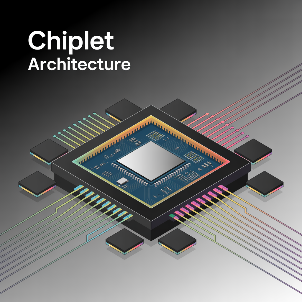
Heterogeneous Integration and Chiplet Architecture
Perhaps the most transformative trend in semiconductor design is the widespread adoption of chiplet architecture and heterogeneous integration. Rather than manufacturing monolithic system-on-chips (SoCs), companies are increasingly designing specialized chiplets that can be combined using advanced packaging technologies.
This approach offers several advantages:
- Improved yield rates and cost efficiency
- Greater design flexibility and customization
- Ability to mix process nodes for optimal performance
- Faster time-to-market for new products
Leading companies have established open standards for chiplet interfaces, fostering an ecosystem where specialized components from different manufacturers can be seamlessly integrated.
AI-Driven Semiconductor Design
Artificial intelligence has transformed the semiconductor design process itself. AI algorithms now assist engineers in optimizing chip layouts, predicting performance characteristics, and identifying potential issues before manufacturing begins.
These AI design tools have dramatically reduced development cycles while improving performance outcomes. In some cases, AI-optimized designs have achieved performance improvements of 15-20% compared to traditional human-designed layouts.
Sustainable Manufacturing Practices
Environmental considerations have become central to semiconductor manufacturing. The industry has made significant strides in reducing water usage, energy consumption, and chemical waste. New facilities are being designed with sustainability as a core principle rather than an afterthought.
Several major manufacturers have committed to carbon-neutral operations by 2030, investing heavily in renewable energy sources and circular economy practices for rare materials recovery.
The Future Outlook
As we look beyond 2025, several emerging technologies promise to further revolutionize the semiconductor landscape:
- Quantum computing integration - Hybrid classical/quantum architectures
- Neuromorphic computing - Brain-inspired chip designs for AI applications
- Advanced materials - Beyond silicon substrates for specialized applications
- 3D integration - Moving beyond 2D planar designs to true 3D architectures
The pace of innovation shows no signs of slowing, with research labs already demonstrating early prototypes of technologies that will define the next decade of electronic systems.
The semiconductor industry's evolution continues to underpin advancements across virtually every sector of the global economy. From smartphones to autonomous vehicles, data centers to medical devices, the innovations happening at the nanoscale are enabling transformative capabilities at the human scale.
As we navigate this exciting technological frontier, collaboration between industry, academia, and government will be essential to addressing the challenges and opportunities that lie ahead.


Comments (5)
Leave a Comment
Michael Chen
May 6, 2025 at 10:45 AMGreat article! I'm particularly interested in the heterogeneous integration approach. Do you think this will lead to more specialized chip designs for specific applications rather than general-purpose processors?
Sarah Williams
May 6, 2025 at 11:30 AMThe sustainability aspect is crucial. I'd love to see more details on how semiconductor manufacturers are addressing their massive water usage, especially in water-stressed regions.
Robert Johnson
May 6, 2025 at 2:15 PMI'm skeptical about the timeline for 2nm commercialization. The challenges with quantum effects at this scale are significant. Has any manufacturer actually demonstrated working chips at this node yet?
Alex Johnson Author
May 6, 2025 at 3:40 PMGreat question, Robert. Yes, there have been working prototypes demonstrated, though mass production is still ramping up. The timeline I've presented reflects the most recent announcements from the major players in the industry.
Lisa Patel
May 7, 2025 at 9:20 AMThe AI-driven design tools section was fascinating. I work in EDA and we're seeing incredible results with these new approaches. Would love to see a follow-up article focused specifically on this topic!